
Researchers developed a new method of processing nanomaterials that could lower the cost of manufacturing thin-film devices.
Engineers from the Rutgers University-New Brunswick and Oregon State Universityhave reportedly developed a new process that will allow intense pulsed light (IPL) sintering to be used at a lower temperature.

Apparently, this would enable low-cost, temperature-sensitive nanomaterials to be used in manufacturing thin-film devices like window coatings and touchscreens.
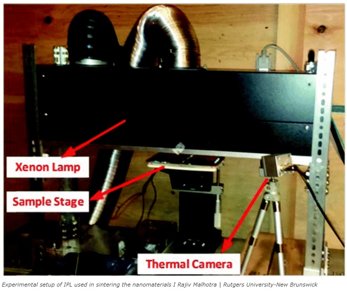
Under normal circumstances, IPL utilizes the “pulsed, large-area, broad-spectrum visible light” coming from a xenon lamp to rapidly fuse nanomaterials into thin films, or in patterns found in solar cells, flexible sensors, displays, and other applications. A nanomaterial is characterized by its tiny size measured by scientists in nanometers.
@RutgerU and @OregonState researchers have developed a new method of processing nanomaterials which could revolutionize the manufacturing of thin-film electronic devices!CLICK TO TWEETHow small is a nanometer?
Well, a nanometer is one-millionth of a millimeter which makes it about 100,000 times smaller than the diameter of human hair. For comparison, an average hair strand has a diameter of about 17 to 181 millionths of a meter.
Apparently, the said conventional method of pulsed light fusion used in processing nanomaterials requires 250 degrees Celsius (over 480 degrees Fahrenheit) of temperature just to combine electricity conducting structures with silver nanospheres.
Using Low Temperature to Process Nanomaterials
In the study published by the researchers in the journal RSC Advances, they used temperatures of 150 to 240 degrees Celsius while doing IPL sintering. During their experiment, they compared the thickness, resistivity, micromorphology, crystallinity, and optical properties of the film utilized in different ratios of its nanowire to nanoparticle content.
With this information, they were able to change the temperature evolution trends over successive pulses while enabling film resistivity within four to five times that of bulk silver. The method allowed them to acquire the said properties just within 2.5 seconds of the processing time.
The success of the experiment reportedly means that the sharp reduction in temperature during fusion will make it possible for low-cost and temperature-sensitive plastic substrates. For example, polyethylene terephthalate (PET) and polycarbonate can be used without compromising process throughput.
“Pulsed light sintering of nanomaterials enables really fast manufacturing of flexible devices for economies of scale,” Rajiv Malhotra, the senior author of the study and assistant professor in the Department of Mechanical and Aerospace Engineering at Rutgers-New Brunswick, said. “Our innovation extends this capability by allowing cheaper temperature-sensitive substrates to be used.”
To date, silver nanomaterials are used in devices like radio-frequency identification (RFID) tags, solar cells, and display devices to conduct electricity. Fusing conductive nanomaterials with flexible substrates like polymers or plastics is required to make flexible forms of the said electronic devices.
“The next step is to see whether other nanomaterial shapes, including flat flakes and triangles, will drive fusion temperatures even lower,” Malhotra went on to say.
In a separate study, the same team of researchers was also able to demonstrate pulsed light sintering of copper sulfide nanoparticles, enabling them to create films that are less than 100 nanometers thick. This, according to the researchers, could speed up the manufacturing of copper sulfide thin films used in window coatings and electronic parts to name a few.
Where else do you think this new method of fusing nanomaterials could be used?
Related Topics